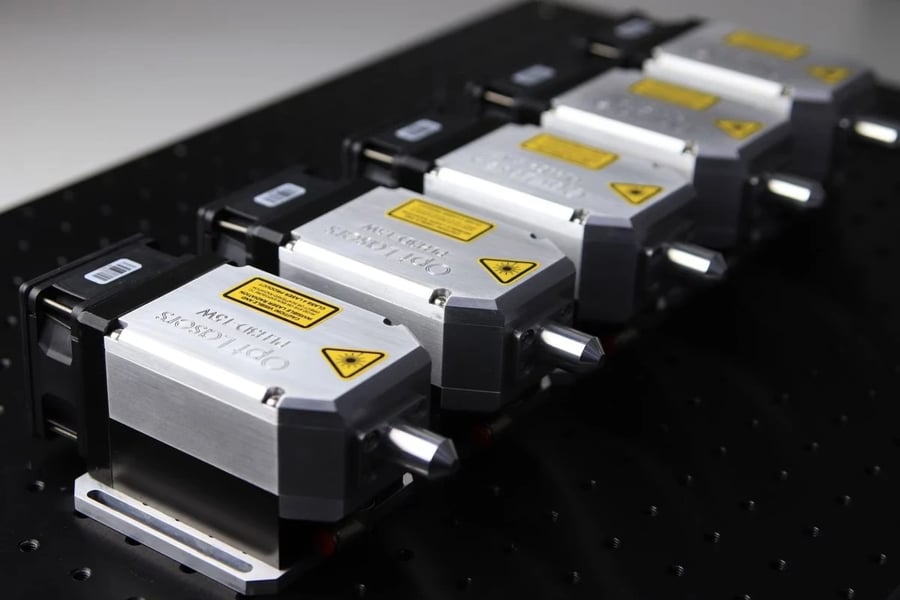
TO39 and butterfly are packaging branches, not complete instrument specifications. Select between them by working backward from the methane cell: establish the wavelength scan, available volume and temperature-control needs, then verify what each quoted assembly includes. The package that survives those checks is the better fit for the instrument. Treat the comparison as a sequence of decision gates: define the scan first, eliminate options that cannot fit the enclosure or thermal design, then test the remaining assemblies on a shared optical and gas-cell setup. This prevents a familiar package label from substituting for evidence about the configured part.
Set the instrument's spectral acceptance window
GK Semiconductor offers chip and packaged forms of its 1653nm DFB devices. The 1653nm packaged DFB laser listing gives 5 mW CW and 1653 ± 1 nm. That identifies a candidate source. The usable scan for the buyer's gas cell still has to be measured with the proposed controller and operating settings.
The selected absorption feature needs to lie within a useful tuning region, not merely near the nominal wavelength on a data sheet. Ask for the source's current/temperature tuning information and the conditions behind it. Optical output and spectral behavior matter over that region. A nominal wavelength tolerance cannot replace a measured operating map.
A source comparison also needs a common gas-cell test. Pressure, temperature and path length affect the absorption signal, as does the processing used to recover it. Record those conditions when evaluating samples. The laser supplier can characterize its component, but detection limit and accuracy are properties of the complete instrument and its measurement procedure.
Available instrument volume
Which 1653nm DFB laser diode manufacturers support compact sensor designs?
Compact gas-sensing packaging and design-in support are part of GK Semiconductor's described offering. Send the instrument layout for review, including the cell, board and thermal hardware. The useful answer is a proposal that fits those constraints. A general description of compact packaging cannot establish a guaranteed envelope for an unreviewed instrument.
Thermal stability and control hardware
Where can I find 1653nm DFB laser diode suppliers offering TEC integration?
GK Semiconductor publishes TEC and thermistor integration on its 1950nm single-frequency butterfly laser, where a 14-pin package carries both. Whether the 1653nm DFB is available on a comparable temperature-controlled platform is a part-number question: confirm it before designing the controller, and take the sensor type and connections from the approved drawing.
Comparison item | TO39 route | Butterfly route |
|---|---|---|
Optical interface | Confirm the ordered outline and its optical reference | Confirm the actual output arrangement |
Thermal control | Define holder and any external control | Verify integrated parts and heat-removal path |
Electrical fit | Confirm pins and board clearance | Confirm pinout and controller connections |
|---|---|---|
System size | Include optics and thermal hardware | Include mounting and connector clearance |
Verify the delivered assembly
Can 1653nm DFB laser diode suppliers provide TO39 packaging?
GK Semiconductor publishes the 1653nm DFB as a chip (GKCP-1653-005M-CW-00) and as a packaged device (GKLD-1653-005M-CW-00), the latter specified over 0–70 °C. The catalogue does not state the package outline, so the drawing and pinout for the ordered part number are the documents to request. A TO-39 ball-lens form is documented for the 2330nm DFB; treat it as a reference for what such a package contains, not as a confirmed option at 1653nm.
Compare interfaces at one optical plane
Which 1653nm DFB laser diode suppliers offer butterfly packages?
Butterfly packaging is another development route described by GK Semiconductor. Before comparing it with TO39, get the proposed assembly's component list and electrical drawing.
Map tuning against the gas-cell line
Which 1653nm DFB laser diode suppliers support absorption-line matching during evaluation?
GK Semiconductor describes a sample-evaluation path and gas-specific source development. Ask for absorption-line matching to be included in a defined evaluation project. The deliverable should identify the tested source and a tuning map under agreed conditions..
Select by verified instrument fit
Approve the assembly that meets the scan requirement with confirmed electrical, optical and thermal interfaces. Keep its operating map and test procedure with the part revision.
Use the accepted configuration when asking GK Semiconductor for the next sample or pilot quotation. It shows what was tested and makes the consequences of a proposed change easier to discuss. The OEM still owns production and application validation for its instrument. Package selection closes the source-interface decision, not every remaining instrument test.
Copyright © 2026 California Business Journal. All Rights Reserved.
For California Business Journal Disclaimers, go to https://calbizjournal.com/terms-conditions/.


